|
|
  |
|
:: 인터플렉스에 오신것을 환영합니다 ::
| |
| |
|
 |
|
|
| |
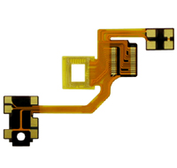
FPC의 가장 기본적인 TYPE으로 connector를
연결하는 cable과 전자제품의 sub board에
사용되는 등 주로 간단한 기능을 가진 제품에
적용된다.
최근에는 fine pattern의 요구에 따른 image
기술의 정도, solder mask의 다양화 등
저부가가치 제품이라는 인식이 변하는 추세이다. |
|
|
| |
|
 |
|
| |
|
| |
|
| |
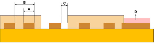
Artwork Design Rules |
| |
| |
Artwork Design Rules |
Low Cost |
High Cost |
|
|
|
|
|
| A |
Line Width |
80 |
70 |
| B |
Line to Line Pitch |
160 |
140 |
| C |
Coverlay Attachment Tolerance |
±150 |
±100 |
| D |
Final Surface |
Electro Ni/Au |
|
| Direct Gold(Electro) |
Min 0.8 |
| Elect Sn/Pb |
2~10 |
| Immersion Tin |
Min 0.4 |
|
| |
|
 |
|
| |
|
| |
|
 |
|
| |
|
|
|
|